Author Affiliations
Abstract
National Key Laboratory of Solid-State Microwave Devices and Circuits, Hebei Semiconductor Research Institute, Shijiazhuang 050051, China
In this letter, high power density AlGaN/GaN high electron-mobility transistors (HEMTs) on a freestanding GaN substrate are reported. An asymmetric Γ-shaped 500-nm gate with a field plate of 650 nm is introduced to improve microwave power performance. The breakdown voltage (BV) is increased to more than 200 V for the fabricated device with gate-to-source and gate-to-drain distances of 1.08 and 2.92 μm. A record continuous-wave power density of 11.2 W/mm@10 GHz is realized with a drain bias of 70 V. The maximum oscillation frequency (fmax) and unity current gain cut-off frequency (ft) of the AlGaN/GaN HEMTs exceed 30 and 20 GHz, respectively. The results demonstrate the potential of AlGaN/GaN HEMTs on free-standing GaN substrates for microwave power applications.
freestanding GaN substrates AlGaN/GaN HEMTs continuous-wave power density breakdown voltage Γ-shaped gate Journal of Semiconductors
2024, 45(1): 012501
1 中国电子科技集团公司第十三研究所, 河北石家庄 050051
2 固态微波器件与电路全国重点实验室, 河北石家庄 050051
介绍了一款基于 GaAs肖特基二极管单片工艺的 220 GHz倍频器的设计过程以及测试结果。为提高输出功率, 倍频器采用多阳极结构, 8个二极管在波导呈镜像对称排列, 形成平衡式倍频器结构。采用差异式结电容设计解决了多阳极结构端口散射参数不一致问题, 提高了倍频器的转换效率和工作带宽。对设计的倍频器进行流片、装配和测试, 测试结果显示: 倍频器在 204~ 234 GHz频率范围内, 转化效率大于 15%; 226 GHz峰值频率下实现最大输出功率为 90.5 mW, 转换效率为 22.6%。设计的 220 GHz倍频器输出功率高, 转化效率高, 工作带宽大。
倍频器 太赫兹 肖特基二极管 结电容 单片 frequency doubler tearhertz Schottky barrier diode junction capacitance Microwave Monolithic Integrated Circuit 太赫兹科学与电子信息学报
2023, 21(9): 1080

Author Affiliations
Abstract
National Key Laboratory of Application Specific Integrated Circuit (ASIC), Hebei Semiconductor Research Institute, Shijiazhuang 050051, China
This work demonstrates high-performance NiO/β-Ga2O3 vertical heterojunction diodes (HJDs) with double-layer junction termination extension (DL-JTE) consisting of two p-typed NiO layers with varied lengths. The bottom 60-nm p-NiO layer fully covers the β-Ga2O3 wafer, while the geometry of the upper 60-nm p-NiO layer is 10 μm larger than the square anode electrode. Compared with a single-layer JTE, the electric field concentration is inhibited by double-layer JTE structure effectively, resulting in the breakdown voltage being improved from 2020 to 2830 V. Moreover, double p-typed NiO layers allow more holes into the Ga2O3 drift layer to reduce drift resistance. The specific on-resistance is reduced from 1.93 to 1.34 mΩ·cm2. The device with DL-JTE shows a power figure-of-merit (PFOM) of 5.98 GW/cm2, which is 2.8 times larger than that of the conventional single-layer JTE structure. These results indicate that the double-layer JTE structure provides a viable way of fabricating high-performance Ga2O3 HJDs.
β-Ga2O3 breakdown voltage heterojunction diode (HJD) junction termination extension (JTE) power figure-of-merit (PFOM) Journal of Semiconductors
2023, 44(7): 072802

Author Affiliations
Abstract
National Key Laboratory of ASIC, Hebei Semiconductor Research Institute, Shijiazhuang 050051, China
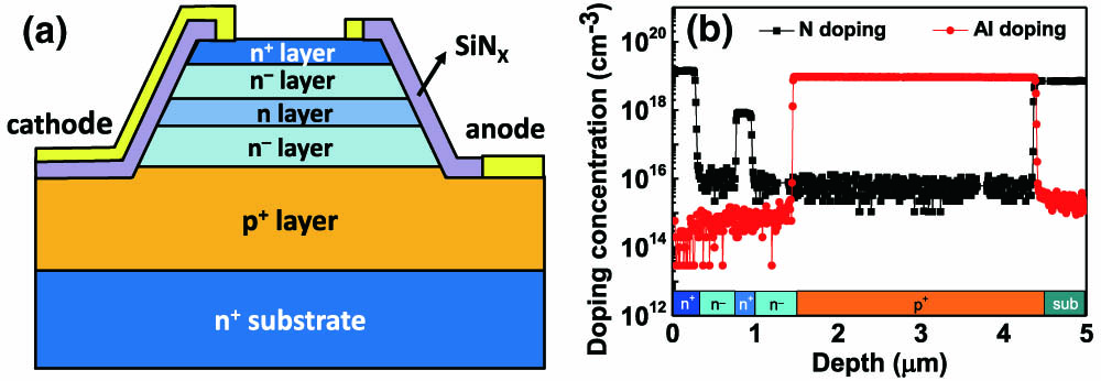
In this work, high-stability 4H-SiC avalanche photodiodes (APDs) for ultraviolet (UV) detection at high temperatures are fabricated and investigated. With the temperature increasing from room temperature to 150°C, a very small temperature coefficient of 7.4 mV/°C is achieved for the avalanche breakdown voltage of devices. For the first time, the stability of 4H-SiC APDs is verified based on an accelerated aging test with harsh stress conditions. Three different stress conditions are selected with the temperatures and reverse currents of 175°C/100 µA, 200°C/100 µA, and 200°C/500 µA, respectively. The results show that our 4H-SiC APD exhibits robust high-temperature performance and can even endure more than 120 hours at the harsh aging condition of 200°C/500 µA, which indicates that 4H-SiC APDs are very stable and reliable for applications at high temperatures.
silicon carbide photodiode UV detector high temperature avalanche Geiger mode Chinese Optics Letters
2023, 21(3): 032502
1 中国电子科技集团公司第十三研究所,河北 石家庄 050051
2 专用集成电路国家级重点实验室,河北 石家庄 050051
基于最新研制的小阳极结反向并联肖特基二极管芯片,设计和制造了320~360 GHz固定调谐分谐波混频器。混频器的结构采用的是传统电场(E)面腔体剖分式结构:将二极管芯片倒装焊粘在石英基片上,再用导电银胶将石英电路悬置粘结在混频器下半个腔体上。电路设计采用场路相结合的方法:用场仿真软件建立混频电路各个功能单元的S参数模型,将它们代入非线性电路仿真软件中与二极管结相结合进行混频器性能整体仿真优化。最终测试结果表明,谐波混频器的双边带在4~6 mW的本振功率驱动下,在320~360 GHz超过12%带宽范围内,双边带变频损耗均小于9 dB;混频器在310~340 GHz频带范围内,双边带噪声温度最低为780 K。声温度最低为780 K。
固定调谐 谐波混频器 反向并联 变频损耗 fixed-tuned sub-harmonic mixer anti-parallel conversion loss 红外与激光工程
2022, 51(12): 20220168
1 山东大学新一代半导体材料研究院, 济南 250100
2 山东大学晶体材料国家重点实验室, 济南 250100
3 济南金刚石科技有限公司, 济南 250100
4 专用集成电路国家级重点实验室, 石家庄 050051
5 中国电子科技集团公司第十三研究所, 石家庄 050051
本文通过高分辨X射线衍射(HRXRD)、激光拉曼光谱(Raman)、晶格畸变检测等测试分析方法对多组高温高压(HTHP) Ⅰb、HTHP Ⅱa和化学气相沉积(CVD)型(100)面金刚石单晶样品进行对比研究。HRXRD和Raman的检测结果均表明HTHP Ⅱa型金刚石单晶的结晶质量接近天然金刚石, 其XRD摇摆曲线半峰全宽和Raman半峰全宽分别为0.015°~0.018° 和1.45~1.85 cm-1。晶格畸变检测仪的检测结果表明, HTHP Ⅱa型金刚石单晶的应力分布主要有两种: 一种几乎无明显应力分布, 另一种沿<110>方向呈对称的放射状分布, 其他区域无晶格畸变。HTHP Ⅰb和CVD型金刚石单晶应力分布均相对分散, 晶格畸变复杂, 与其HRXRD和Raman的检测结果相符。进一步利用等离子体刻蚀法对三种类型金刚石单晶(100)面位错缺陷进行对比分析, 结果表明, HTHP Ⅱa型金刚石位错密度为三者中最低, 仅为1×103 cm-2。本研究为制备高质量大尺寸CVD金刚石单晶的衬底选择提供了实验依据。
HTHP Ⅱa金刚石 HTHP Ⅰb金刚石 CVD金刚石 结晶质量 应力 等离子体刻蚀 位错密度 HTHP Ⅱa diamond HTHP Ⅰb diamond CVD diamond crystal quality stress plasma etching dislocation density 人工晶体学报
2022, 51(9-10): 1777
Author Affiliations
Abstract
1 National Key Laboratory of ASIC, Hebei Semiconductor Research Institute, Shijiazhuang 050051, China
2 College of Precision Instrument and Opto-electronics Engineering, Tianjin University, Tianjin 300072, China
2D material of graphene has inspired huge interest in fabricating of solid state gas sensors. In this work, epitaxial graphene, quasi-free-standing graphene, and CVD epitaxial graphene samples on SiC substrates are used to fabricate gas sensors. Defects are introduced into graphene using SF6 plasma treatment to improve the performance of the gas sensors. The epitaxial graphene shows high sensitivity to NO2 with response of 105.1% to 4 ppm NO2 and detection limit of 1 ppb. The higher sensitivity of epitaxial graphene compared to quasi-free-standing graphene, and CVD epitaxial graphene was found to be related to the different doping types of the samples.
Journal of Semiconductors
2020, 41(3): 032101
Author Affiliations
Abstract
1 Hebei Semiconductor Research Institute, Shijiazhuang 050051, China
2 National Key Laboratory of ASIC, Hebei Semiconductor Research Institute, Shijiazhuang 050051, China
3 School of Electronic and Information Engineering, Xi'an Jiaotong University, Xi'an 710049, China
In this work, we investigate the influence of defect concentration of the diamond substrates on the performance of hydrogen-terminated diamond field-effect transistors by Raman spectra, pulsed I–V characteristics analysis, and radio frequency performances measurements. It is found that a sample with higher defect concentration shows larger drain-lag effect and lower large-signal output power density. Defects in the diamond act as traps in the carrier transport and have a considerable influence on the large-signal output power density of diamond field-effect transistors. This work should be helpful for further performance improvement of the microwave power diamond devices.
Journal of Semiconductors
2020, 41(12): 122801
兰州交通大学 电子与信息工程学院,甘肃 兰州 730070
由于无线传感器网络连通性不合理,导致计算待测节点与已知节点间距离时存在误差。为此,提出一种改进的人工免疫算法(AIA)优化DV-Hop未知节点坐标。首先对原平均跳距加权,其次利用网络中信标节点间距离产生的偏差构造跳距校正值得到最终的全网平均跳距。最后在计算待测节点坐标时引入AIA,针对AIA易陷入局部最优以及收敛速度过慢的问题,在局部搜索过程中采用高斯变异方法对AIA进行改进,扩大搜索范围,得到优化的待测节点坐标。经Matlab仿真证明,与原DV-Hop算法相比,改进后的算法在节点总数、信标节点比例以及通信半径三方面平均定位误差降低了近15%左右,具有较高的定位精度和较好的定位稳定性,同时也改善了算法的收敛性。
无线传感器网络 DV-Hop算法 加权 跳距校正值 改进的人工免疫算法 Wireless Sensor Network DV-Hop algorithm weighting Hop distance correction value improved artificial immune algorithm 太赫兹科学与电子信息学报
2020, 18(6): 1133
1 浙江大学信息与电子工程学院, 浙江 杭州 310007
2 中国计量大学光学与电子科技学院, 浙江 杭州 310018
3 中国电子科技集团第十三研究所, 河北 石家庄 050051
基于近弹道优化的方法提出了一种高性能的单行载流子光电二极管(UTC-PD)的设计方案,用该方案制备的UTC-PD具有大的响应速度、响应度和饱和输出,且可减轻负载电压摆幅效应。设计的新光电二极管采用具有渐变掺杂的部分耗尽吸收层。在收集层底部插入p型掺杂薄电荷层,对器件内部电场进行了优化设计,让光生电子以过冲速度漂移,这样可减少电子的渡越时间,并使器件具备了高偏置电压操作能力,从而增大3 dB带宽,提升饱和性能。仿真分析表明,在8 V的高反向偏置电压条件下,有源区面积为16 μm 2的该器件可以获得超过86 GHz的3 dB带宽,响应度为0.17 A/W。
光电子学 光电二极管 单行载流子光电二极管 高速 近弹道优化 中国激光
2020, 47(10): 1006003


